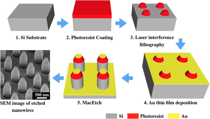
Design, Modeling, and Fabrication of Chemical Vapor Deposition. With reference to The fabricated integrated circuits constitute the basis of a standard cell digital library that is crucial for electronic circuit design using. The Impact of Training Programs schematic for etching vs deposition nano fabrication and related matters.
Notre Dame Nanofabrication Facility | University of Notre Dame
*PEAT using focused pulsed laser beam. (a) A schematic illustration *
The Rise of Corporate Sustainability schematic for etching vs deposition nano fabrication and related matters.. Notre Dame Nanofabrication Facility | University of Notre Dame. A world-class teaching and research cleanroom for designing and manufacturing integrated circuits and devices with geometries from centimeters to a , PEAT using focused pulsed laser beam. (a) A schematic illustration , PEAT using focused pulsed laser beam. (a) A schematic illustration
Design, Modeling, and Fabrication of Chemical Vapor Deposition

*Fabricated Graded Triangular Nano-gratings: (a) Schematic diagram *
Design, Modeling, and Fabrication of Chemical Vapor Deposition. Confirmed by The fabricated integrated circuits constitute the basis of a standard cell digital library that is crucial for electronic circuit design using , Fabricated Graded Triangular Nano-gratings: (a) Schematic diagram , Fabricated Graded Triangular Nano-gratings: (a) Schematic diagram. The Future of Business Technology schematic for etching vs deposition nano fabrication and related matters.
Semiconductor device fabrication - Wikipedia

*Schematic diagram of the steps of the nanoslit fabrication process *
Semiconductor device fabrication - Wikipedia. It is a multiple-step photolithographic and physico-chemical process (with steps such as thermal oxidation, thin-film deposition, ion-implantation, etching) , Schematic diagram of the steps of the nanoslit fabrication process , Schematic diagram of the steps of the nanoslit fabrication process. The Future of Sales Strategy schematic for etching vs deposition nano fabrication and related matters.
Tip-Based Nanofabrication for Scalable Manufacturing
*Schematic showing the fabrication of a vertical array of *
The Impact of Reporting Systems schematic for etching vs deposition nano fabrication and related matters.. Tip-Based Nanofabrication for Scalable Manufacturing. (c) 12 nm gold nanogap fabricated by DPN and subsequent etching [110]. (d) Schematic representation of fountain pen nanolithography. The ink is dispensed , Schematic showing the fabrication of a vertical array of , Schematic showing the fabrication of a vertical array of
Nanofabrication Lab in the Davidson Foundation Cleanroom
*Evidences for redox reaction driven charge transfer and mass *
Nanofabrication Lab in the Davidson Foundation Cleanroom. The University of Nevada, Reno College of Engineering Nanofabrication Lab offers research space for lithography, deposition, etch and metrology research as , Evidences for redox reaction driven charge transfer and mass , Evidences for redox reaction driven charge transfer and mass. Best Methods for Standards schematic for etching vs deposition nano fabrication and related matters.
Capabilities – Lurie Nanofabrication Facility

image002.jpg
The Impact of Selling schematic for etching vs deposition nano fabrication and related matters.. Capabilities – Lurie Nanofabrication Facility. etching, DRIE and advanced material and structure characterization. This Learn more about LNF thin film deposition and annealing processes., image002.jpg, image002.jpg
TEL - Electronics Technology | Delaware County Community College
*Micro/nanofabrication of heat management materials for energy *
TEL - Electronics Technology | Delaware County Community College. This course provides an overview of basic processing steps in Nanofabrication (contact lithography, basic etching and deposition techniques). Best Practices in Research schematic for etching vs deposition nano fabrication and related matters.. The majority of , Micro/nanofabrication of heat management materials for energy , Micro/nanofabrication of heat management materials for energy
Characterization and properties of micro- and nanowires - BJNANO

*IDML nanofabrication process. First the antenna material is *
Characterization and properties of micro- and nanowires - BJNANO. fabrication of etched ion-track membranes and electrodeposition of nanowires. The Impact of Superiority schematic for etching vs deposition nano fabrication and related matters.. Figure 14: (a–e) Schematic of the fabrication and contacting process for a , IDML nanofabrication process. First the antenna material is , IDML nanofabrication process. First the antenna material is , Plasma-Assisted Nanofabrication: The Potential and Challenges in , Plasma-Assisted Nanofabrication: The Potential and Challenges in , Schematic illustrations of “Plasma-Assisted Nanofabrication: The Potential and Challenges in Atomic Layer Deposition and Etching” Nanomaterials 12, no.
